Why it matters: Many believe that glass substrate technology will enable the industry to sustain Moore’s Law beyond 2030, ensuring continuous development without being constrained by process size limitations. Samsung aims to outpace Intel, which has been researching glass substrates for nearly a decade and intends to incorporate them into commercial products by 2030. With its updated timeline, the South Korean conglomerate stands a good chance of launching its products ahead of Intel.
Samsung Electro-Mechanics is accelerating its efforts in the semiconductor glass substrate market by advancing its equipment procurement and installation activities to September. According to ETNews, it will also launch a pilot line for its next-gen packaging in Sejong, South Korea, in the fourth quarter – one quarter ahead of schedule.
Earlier this year, the subsidiary initiated R&D work on glass substrates and started exploring potential use cases.
While Samsung hinted at the future of glass substrates during CES 2024, it now appears that the South Korean conglomerate is moving forward more swiftly to gain a competitive edge, particularly against Intel. Samsung now anticipates commencing production of glass substrates for high-end system-in-packages in 2026.
The company has finalized its list of suppliers for the projects, selecting Philoptics, Chemtronics, Joongwoo M-Tech, and Germany’s LPKF to provide components.

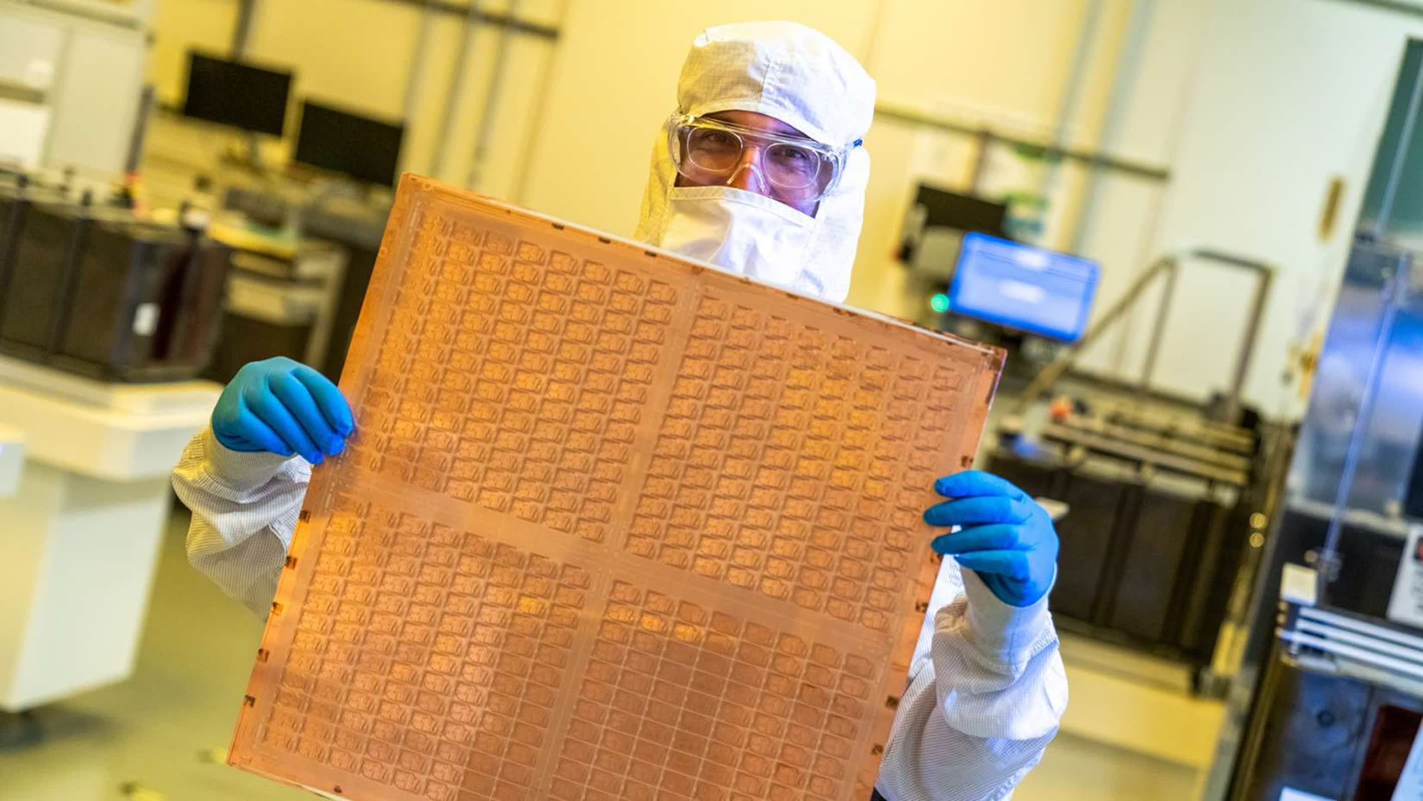
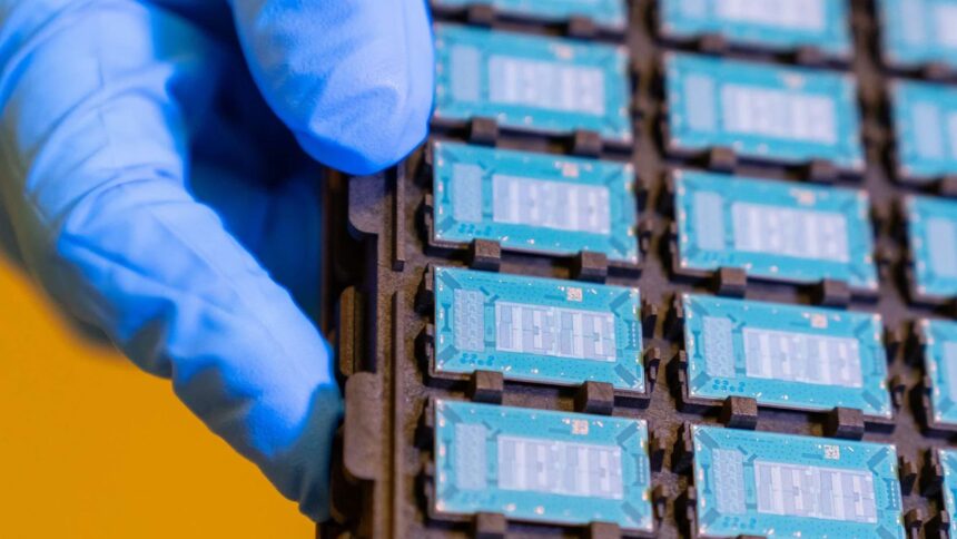
Glass substrate holds considerable promise for advancing the scaling of transistors in semiconductor packages. Intel forecasts that by the end of the decade, the semiconductor industry will hit its limits in scaling transistors on silicon packages using organic substrates due to their higher power consumption, susceptibility to shrinkage, and warping.
In contrast, glass offers ultra-low flatness, enabling components to be placed closer together, along with superior thermal and mechanical stability, leading to significantly higher interconnect density in substrates, potentially up to a 10x increase. These advantages empower chip architects to design high-density, high-performance chip packages suited for data-intensive tasks like artificial intelligence.
Apple is also exploring the potential of glass substrate and reportedly engaging in discussions with various suppliers, including likely Samsung, to develop a strategy for integrating glass substrates into electronic devices.
However, several challenges lie ahead, including the need to address integration and interface engineering issues, as highlighted by Rahul Manepalli, fellow and director of substrate TD module engineering at Intel. Other obstacles include fragility, inadequate adhesion to metal wires, and difficulties in achieving uniform via fill, crucial for consistent electrical performance.
Nevertheless, optimism prevails regarding resolving these challenges. The global glass substrate market is projected to reach $2.3 billion this year and is expected to witness a robust compound annual growth rate (CAGR) of 5.9 percent from 2024 to 2034, with market revenue for glass substrate anticipated to reach $4.2 billion by 2034.

